- 您现在的位置:买卖IC网 > Sheet目录493 > NTZD3154NT5G (ON Semiconductor)MOSFET N-CHAN DUAL 20V SOT-563
�� �
�
�NTZD3154N�
�Small� Signal� MOSFET�
�20� V,� 540� mA,� Dual� N� ?� Channel�
�Features�
�?�
�?�
�?�
�?�
�?�
�Low� R� DS(on)� Improving� System� Efficiency�
�Low� Threshold� Voltage�
�Small� Footprint� 1.6� x� 1.6� mm�
�ESD� Protected� Gate�
�These� Devices� are� Pb� ?� Free,� Halogen� Free/BFR� Free� and� are� RoHS�
�Compliant�
�V� (BR)DSS�
�20�
�http://onsemi.com�
�R� DS(on)� Typ� I� D� Max� (Note� 1)�
�400� m� W� @� 4.5� V�
�500� m� W� @� 2.5� V� 540� mA�
�700� m� W� @� 1.8� V�
�Applications�
�?� Load/Power� Switches�
�?� Power� Supply� Converter� Circuits�
�?� Battery� Management�
�?� Cell� Phones,� Digital� Cameras,� PDAs,� Pagers,� etc.�
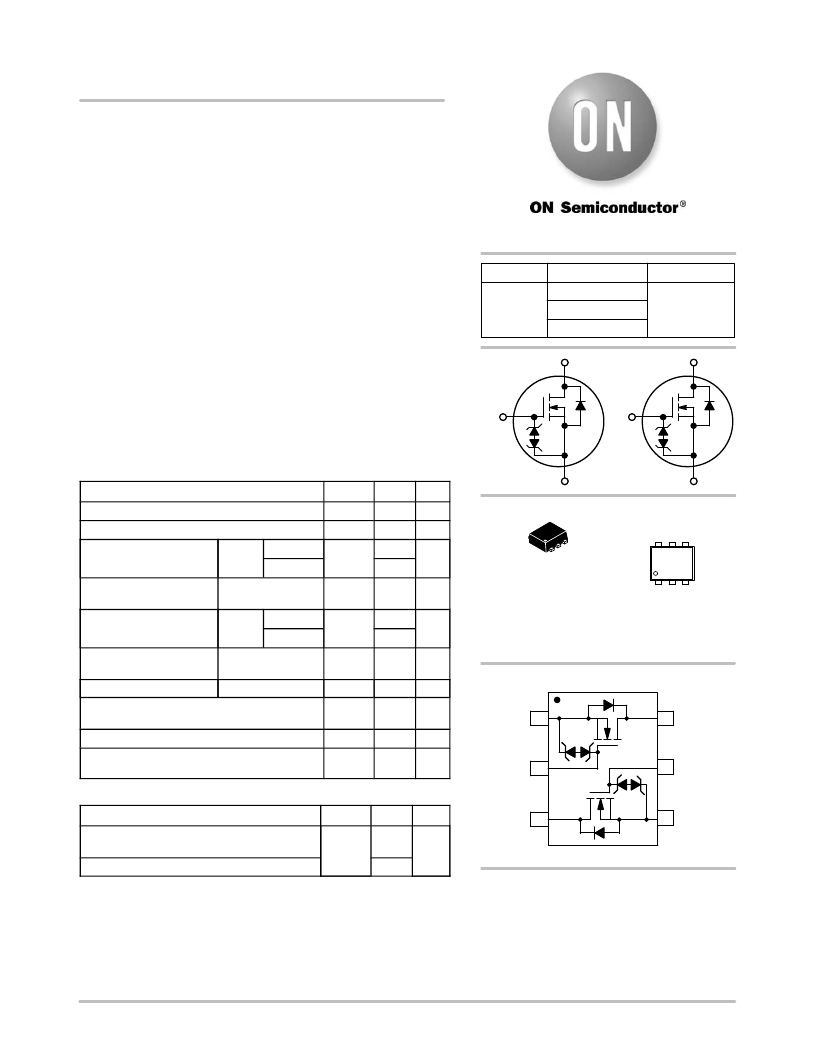
�G1�
�D1�
�G2�
�D2�
�MAXIMUM� RATINGS� (T� J� =� 25� °� C� unless� otherwise� noted.)�
�Parameter� Symbol�
�Value�
�Unit�
�S1�
�N� ?� Channel�
�MOSFET�
�S2�
�T� A� =� 85� °� C�
�Drain� ?� to� ?� Source� Voltage�
�Gate� ?� to� ?� Source� Voltage�
�Continuous� Drain� Current�
�(Note� 1)�
�Power� Dissipation�
�(Note� 1)�
�Continuous� Drain� Current�
�(Note� 1)�
�Power� Dissipation�
�(Note� 1)�
�Pulsed� Drain� Current�
�Steady� T� A� =� 25� °� C�
�State�
�Steady� State�
�T� A� =� 25� °� C�
�t� v� 5s�
�T� A� =� 85� °� C�
�t� v� 5s�
�t� p� =� 10� m� s�
�V� DSS�
�V� GS�
�I� D�
�P� D�
�I� D�
�P� D�
�I� DM�
�20�
�±� 6.0�
�540�
�390�
�250�
�570�
�410�
�280�
�1.5�
�V�
�V�
�mA�
�mW�
�mA�
�mW�
�A�
�MARKING�
�DIAGRAM�
�6�
�1� TV� M� G�
�SOT� ?� 563� ?� 6� G�
�CASE� 463A�
�TV� =� Specific� Device� Code�
�M� =� Date� Code�
�G� =� Pb� ?� Free� Package�
�(Note:� Microdot� may� be� in� either� location)�
�PINOUT:� SOT� ?� 563�
�Operating� Junction� and� Storage� Temperature�
�Source� Current� (Body� Diode)�
�Lead� Temperature� for� Soldering� Purposes�
�(1/8� ″� from� case� for� 10� s)�
�T� J� ,�
�T� STG�
�I� S�
�T� L�
�?� 55� to�
�150�
�350�
�260�
�°� C�
�mA�
�°� C�
�S� 1� 1�
�G� 1� 2�
�6� D� 1�
�5� G� 2�
�THERMAL� RESISTANCE� RATINGS�
�Parameter�
�Junction� ?� to� ?� Ambient� –� Steady� State�
�(Note� 1)�
�Junction� ?� to� ?� Ambient� –� t� v� 5� s� (Note� 1)�
�Symbol�
�R� q� JA�
�Max�
�500�
�447�
�Unit�
�°� C/W�
�D� 2�
�3�
�Top� View�
�4� S� 2�
�Stresses� exceeding� Maximum� Ratings� may� damage� the� device.� Maximum�
�Ratings� are� stress� ratings� only.� Functional� operation� above� the� Recommended�
�Operating� Conditions� is� not� implied.� Extended� exposure� to� stresses� above� the�
�Recommended� Operating� Conditions� may� affect� device� reliability.�
�1.� Surface� mounted� on� FR4� board� using� 1� in� sq� pad� size�
�(Cu.� area� =� 1.127� in� sq� [1� oz]� including� traces).�
�ORDERING� INFORMATION�
�See� detailed� ordering� and� shipping� information� in� the� package�
�dimensions� section� on� page� 4� of� this� data� sheet.�
�?� Semiconductor� Components� Industries,� LLC,� 2013�
�January,� 2013� ?� Rev.� 2�
�1�
�Publication� Order� Number:�
�NTZD3154N/D�
�发布紧急采购,3分钟左右您将得到回复。
相关PDF资料
NTZD3155CT2G
MOSFET N/P-CH COMPL 20V SOT-563
NTZD3156CT5G
MOSFET N/P-CH 20V SOT-563
NTZD5110NT5G
MOSFET N-CH DUAL 60V SOT563
NTZS3151PT5G
MOSFET P-CH 20V 860MA SOT-563
NV06P00472J--
THERMISTOR NTC DISK 4.7KOHM 5%
NVB25P06T4G
MOSFET P-CH 60V 27.5A D2PAK
NVB6410ANT4G
MSOFET N-CH 100V 76A D2PAK
NVD4815NT4G
MOSFET N-CH 30V 6.9A DPAK-4
相关代理商/技术参数
NTZD3155C
制造商:ONSEMI 制造商全称:ON Semiconductor 功能描述:Small Signal MOSFET Complementary 20 V, 540 mA / -430 mA, with ESD protection, SOT-563 package.
NTZD3155CT1G
功能描述:MOSFET 20V 540mA/-430mA Complementary w/ESD RoHS:否 制造商:STMicroelectronics 晶体管极性:N-Channel 汲极/源极击穿电压:650 V 闸/源击穿电压:25 V 漏极连续电流:130 A 电阻汲极/源极 RDS(导通):0.014 Ohms 配置:Single 最大工作温度: 安装风格:Through Hole 封装 / 箱体:Max247 封装:Tube
NTZD3155CT1G
制造商:ON Semiconductor 功能描述:DUAL N/P CH MOSFET 20V SOT-563 制造商:ON Semiconductor 功能描述:DUAL N/P CH MOSFET, 20V, SOT-563
NTZD3155CT1H
制造商:ON Semiconductor 功能描述:COMP SOT563 20V 540MA TR - Tape and Reel 制造商:ON 功能描述:COMP SOT563 20V 540MA TR
NTZD3155CT2G
功能描述:MOSFET COMP 540mA 20V RoHS:否 制造商:STMicroelectronics 晶体管极性:N-Channel 汲极/源极击穿电压:650 V 闸/源击穿电压:25 V 漏极连续电流:130 A 电阻汲极/源极 RDS(导通):0.014 Ohms 配置:Single 最大工作温度: 安装风格:Through Hole 封装 / 箱体:Max247 封装:Tube
NTZD3155CT5G
功能描述:MOSFET 20V 540mA/-430mA Complementary w/ESD RoHS:否 制造商:STMicroelectronics 晶体管极性:N-Channel 汲极/源极击穿电压:650 V 闸/源击穿电压:25 V 漏极连续电流:130 A 电阻汲极/源极 RDS(导通):0.014 Ohms 配置:Single 最大工作温度: 安装风格:Through Hole 封装 / 箱体:Max247 封装:Tube
NTZD3156C
制造商:ONSEMI 制造商全称:ON Semiconductor 功能描述:Small Signal MOSFET
NTZD3156CT1G
功能描述:MOSFET 20/6V Comp w/100K G-S Resistors RoHS:否 制造商:STMicroelectronics 晶体管极性:N-Channel 汲极/源极击穿电压:650 V 闸/源击穿电压:25 V 漏极连续电流:130 A 电阻汲极/源极 RDS(导通):0.014 Ohms 配置:Single 最大工作温度: 安装风格:Through Hole 封装 / 箱体:Max247 封装:Tube